By Michael Alexander and Thomas Kirschstein
The recently announced “European initiative on processors and semiconductor technologies” has bold aims to get the EU semiconductor industry back on its feet. But even with its promised EUR 145 billion of investment, it can’t do it alone. Here we examine the initiative itself, assess action areas and explain why we think the key to success lies in forming non-EU partnerships to enable knowledge transfer.
In December 2020, 19 European Union member states signed off the “European initiative on processors and semiconductor technologies” in a bid to re-establish the EU as a global powerhouse in the semiconductor industry. The joint declaration aims to enhance cooperation and increase investment in equipment and materials, design, and advanced manufacturing and packaging, pledging EUR 145 billion in support.
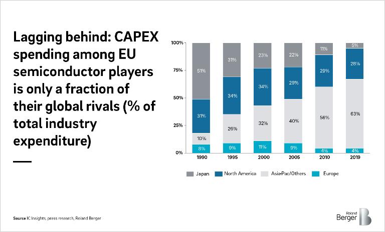
The move comes at a critical time. EU semiconductor producers have long been losing ground to rivals outside the bloc, with leading global players now able to produce smaller and more advanced chips. In addition, the European semiconductor industry’s CAPEX spending has stagnated at around 4% of total expenditure (Asia-Pacific: 63% in 2019). Action is needed, and not just through the initiative or increased CAPEX spending.
In this article, we consider three areas of action, and make a recommendation, that are key to the future success of the EU semiconductor industry. The first is how the industry can leverage one of its main strengths, namely its solid grounding in the manufacture/design of conventional industrial semiconductor products. The second is how the industry can maintain a critical mass, while the third examines how the EU’s new initiative can help to sustain this base. Lastly, we outline why we believe partnering with non-EU technology players is the key to success for EU semiconductor producers.
A strong base to build on
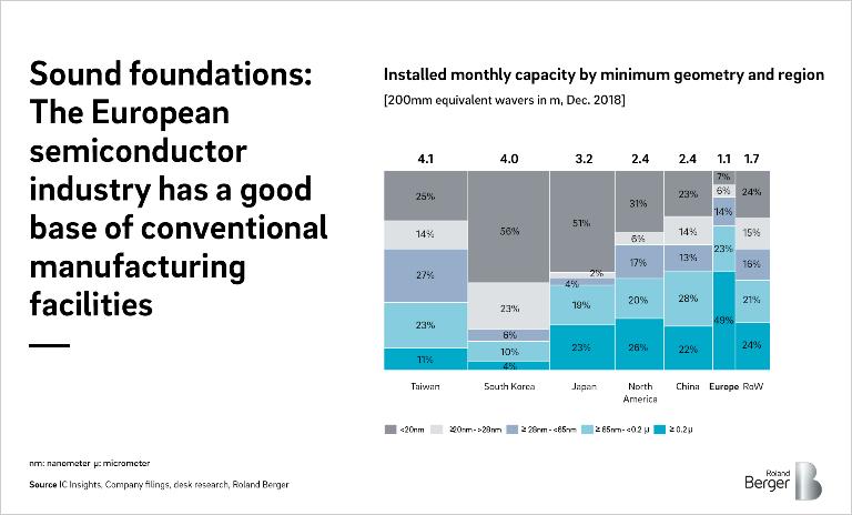
The EU has a solid base in the manufacture, design and research of established technology nodes, and this can be leveraged to rebuild its semiconductor industry. In manufacturing, 49% of all installed capacity is for nodes of ≥0.2 micrometers, the highest share in the world. This ensures a strong base to build on and availability of skilled labor for a manufacturing scale-up. Key production centers in the EU and European Free Trade Association (EFTA) include Austria, France, Germany, Italy, Ireland and the Netherlands, all of which are home to several leading manufacturers.
The EU and EFTA is also home to leading specialized application integrated device manufacturers, with highly competitive players in analog and microcontroller applications, in particular. This will be key to attracting talent.
Regarding research, the EU has a strong research footprint focused on small and medium batch sizes of 100mm and 200mm wafers. Key centers include Fraunhofer in Germany, IMEC in Belgium and CEA-Leti in France. They will play a key role in scaling up the EU R&D effort required to meet the goals of the EU’s initiative.
“The EU needs to re-establish itself as a global semiconductor powerhouse – Even with a funding of EUR 145 bn this goal can only be achieved if the project is realized together with non-EU technology partners.”
Why a critical mass is essential to survival
The initiative states that the EU needs a broader semiconductor base to ensure long-term competitiveness, and we agree. Logic and memory capability will be key for future competitiveness, but the EU currently lacks capability and scale in this area. Achieving critical mass will require two things: safeguarding industrial/automotive innovation , and safeguarding the semiconductor industry itself.
The latest breakthrough innovations heavily depend on semiconductors at current technology nodes (7 nanometers and 5 nanometers). This is particularly the case for the EU’s large and successful automotive and machinery sectors, where AI and autonomous driving applications are driving demand for semiconductors. With industry accounting for 24.6% of the eurozone’s GDP, the need to safeguard its survival is clear.
Currently, most 7nm and 5nm semiconductors are produced in Taiwan and South Korea. But reliance on these non-EU countries carries significant risk. Taiwan is highly prone to earthquakes, with a major seismic event every five years on average. In 1999, for example, a quake with a magnitude of 7.6 on the Richter scale led to a production loss of 20% of monthly output. The country is also caught up in a global trade dispute that could affect its ability to fulfill long-term delivery commitments. These risks need to be mitigated.
The need to safeguard the European industry is accelerated by the recent trend away from x86 processors to ARM-based processors. Infrastructure in the EU is geared towards production of x86-based chips, leaving it further exposed to reliance on non-EU players. This competency deficit is exacerbated by Britain’s departure from the bloc, as ARM is headquartered in the country. Significant skills and IP in central processor and system-on-a-chip architecture have been lost as a result.
How the EU’s semiconductor initiative can help
A key aim of the initiative is to allow EU semiconductor producers to regain competitiveness and catch up with global players.
EU semiconductor CAPEX has been at a low level – between 3% and 4% of total industry expenditure – since the 2009 bankruptcy of German chip-maker Qimonda and the recent move to fab-lite business models (outsourced manufacturing). Increasing this figure is key to improving the EU industry’s level of competitiveness, but commercial players alone do not have the resources to do so. To address this, the initiative pledges EUR 145 billion of state support.
The reason for state intervention is clear. In 2019, the top five global semiconductor CAPEX spenders, which are all based outside the EU, accounted for 69% of all semiconductor CAPEX. This is equivalent to USD 71.2 billion. Such consolidation and huge spending cannot be matched by individual EU players without state backing.
The success of the initiative will ultimately depend on implementation by signatory member states, but we are confident that a coordinated response can enable EU chipmakers to close the CAPEX gap.
Recommendation: Partner with non-EU technology players
To complement the investment support, we recommend that EU semiconductor producers partner with a non-EU technology player. Working together, partners can shorten technology development timelines and ensure better access to R&D resources.
In development, the typical timeline for moving from 14nm to 7nm nodes is three to five years. But in their current state, it is unrealistic that EU players will reach 7nm capability by 2023-2025 without partnerships. In addition, leading global producers are already working on 3nm and 2nm nodes. This threatens to leave EU players even further behind despite the promised investment.
The R&D gains of partnerships are equally beneficial. For example, leading suppliers are currently hiring huge numbers of highly qualified staff; TSMC announced plans in August 2020 to hire 8,000 engineers to work on 2nm technology. A partnership with a market leader would therefore provide quick access to top-level talent.
Such examples highlight that technology transfer from non-EU partners is just as important as financial support. Indeed, the EU’s EUR 145 billion investment package will be ineffective without such partnerships. But combined, the two prongs of financial support and productive partnerships with non-EU players will ensure that the EU semiconductor industry can re-establish itself as a global powerhouse and safeguard Europe’s industrial innovation .

